


Semiconductors &Nanotechnology:Principles and Applications
Semiconductor and Nanotechnology:A Brief Overview
Semiconductors and nanotechnology are two intertwined fields that have revolutionized technology. While both focus on manipulating materials at the atomic level, they have distinct roles:
Halvledere:
* Hvad er de: Materials with conductivity between that of a conductor and an insulator. They allow controlled flow of electrons, making them ideal for building electronic components.
* Sådan fungerer de: Semiconductors like silicon and germanium have their conductivity altered by adding impurities (doping). This creates "n-type" (excess electrons) and "p-type" (electron "holes") materials. Combining these creates junctions that control electron flow based on applied voltage, forming transistors, diodes, and other components.
* Applikationer: Semiconductors are the foundation of modern electronics, powering everything from computers and smartphones to cars and medical devices.
Nanoteknologi:
* Hvad det er: The manipulation of matter on an atomic and molecular scale, typically 1-100 nanometers.
* Sådan virker det: Nanomaterials have unique properties compared to bulk materials due to their increased surface area and quantum effects. These properties can be controlled by manipulating size, shape, and composition at the nanoscale.
* Applikationer: Nanotechnology is being explored in various fields:
* Medicin: Targeted drug delivery, diagnostic tools, tissue engineering
* Elektronik: Smaller and faster transistors, high-density data storage
* Energi: Solceller, batterier, brændselsceller
* Materialer: Stronger and lighter materials, self-cleaning surfaces
Forbindelsen:
* Semiconductors are a key area of nanotechnology research. Ved at kontrollere størrelsen og strukturen af halvledermaterialer på nanoskala kan videnskabsmænd skabe endnu mere effektive og kraftfulde elektroniske enheder.
* Nanoteknologi bruges også til at skabe nye halvledermaterialer med forbedrede egenskaber, såsom forbedret ledningsevne eller bedre lysabsorption.
Eksempler:
* Transistorer: The foundation of modern electronics, getting smaller and more powerful thanks to nanotechnology advancements.
* Kvanteprikker: Tiny semiconductor crystals with controllable light emission, used in displays, lasers, and biological imaging.
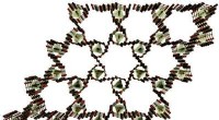
* Graphene: Et enkelt lag af kulstofatomer, der udviser enestående ledningsevne og styrke, med potentielle anvendelser inden for fleksibel elektronik, sensorer og energilagring.
Udfordringer og fremtidige retninger:
* Produktionsudfordringer: Scaling down to the nanoscale requires precise control and specialized equipment.
* Miljøhensyn: The long-term impact of nanomaterials on human health and the environment needs further research.
* Etiske overvejelser: The potential for powerful new technologies raises ethical questions about safety, privacy, and equitable access.
Both semiconductors and nanotechnology are rapidly evolving fields with immense potential to shape the future of technology. Their continued development promises breakthroughs in medicine, energy, materials science, and many other areas.
 Varme artikler
-
 Nanosvamp filtrerer herbicidgifte fraEn ny organisk metalramme kan effektivt filtrere toksiner fra vand. (Phys.org) — Ny forskning har vist potentialet i en ny slags nanomateriale til at filtrere miljøgifte fra vand. Et team af fors
 -
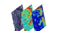 Forskere undersøger kemi, topografi og mekanik med ét instrumentTil en 500-nanometer dyb polymer tynd film fremstillet af polystyren (lysere) og poly-2-vinylpyridin (mørkere), et multimodalt instrument afbildet, fra venstre, overfladetopografi, bulkmaterialets ela
 -
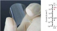 Plastprodukter kunne nemt blive elektroniske med de første formbare kredsløb i kulstof(Venstre) Enhed udelukkende i carbon fremstillet på et fleksibelt polymersubstrat. (Højre) ON- og OFF-strømmene for transistoren i udelukkende kulstof til forskellige bøjningsniveauer. Kredit:Sun, et
 -
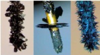 Elektrokrystallisering - gennembrud inden for guld -nanopartikelforskningKredit:University of Jyväskylä Et forskerhold ledet af professor Flavio Maran fra University of Padova (Italien) og akademiprofessor Kari Rissanen fra University of Jyväskylä (Finland) har offentl
- Hvilket instrument måler varm eller kold luft?
- ESA booster opstart til Månen
- Mere end 1,1 million havskildpadder pocheret i løbet af de sidste tre årtier:undersøgelse
- Googles grønne energikøb øger CO2-fri portefølje
- Ny sub-Saturn-masse exoplanet opdaget
- Hvordan kan jeg verificere ægtheden af formørkelsesglas?